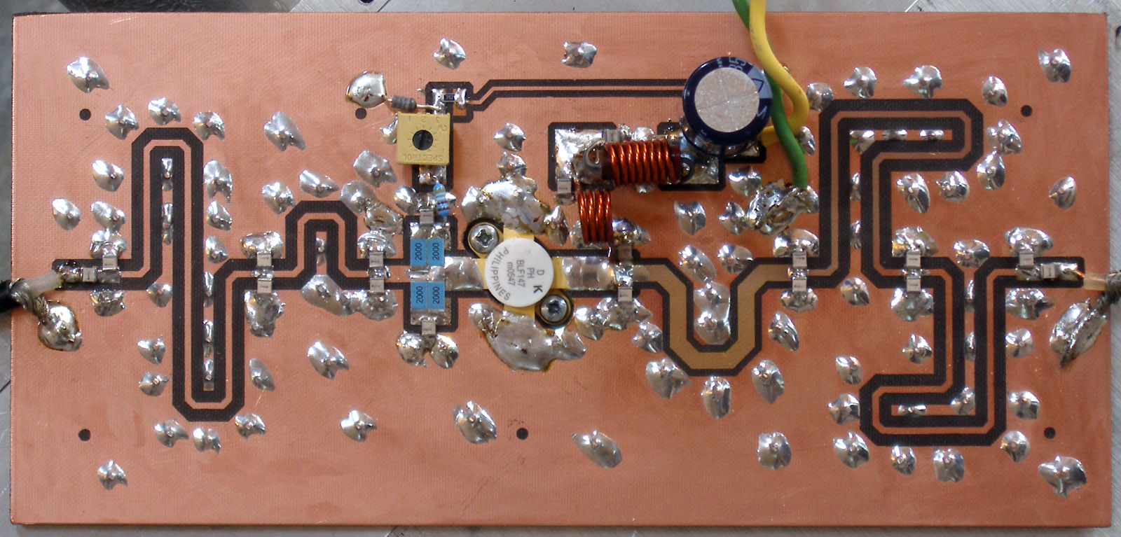
One of the very latest developments here at G-Cipher Laboratories - 150
W across the
band with a BLF147 on 24 VDC, 0.060" Teflon/Glass
board
(dk =
2.50), printed
transmission lines, and ATC 100B porcelain caps. Makes 200 W with a 28
V supply, but best to run it at 24 V or below to be sane. No external
harmonic filter is needed, as the filtering is built into the matching
network - harmonics are typically < -50 dBc. To be used for research
purposes only, of course.
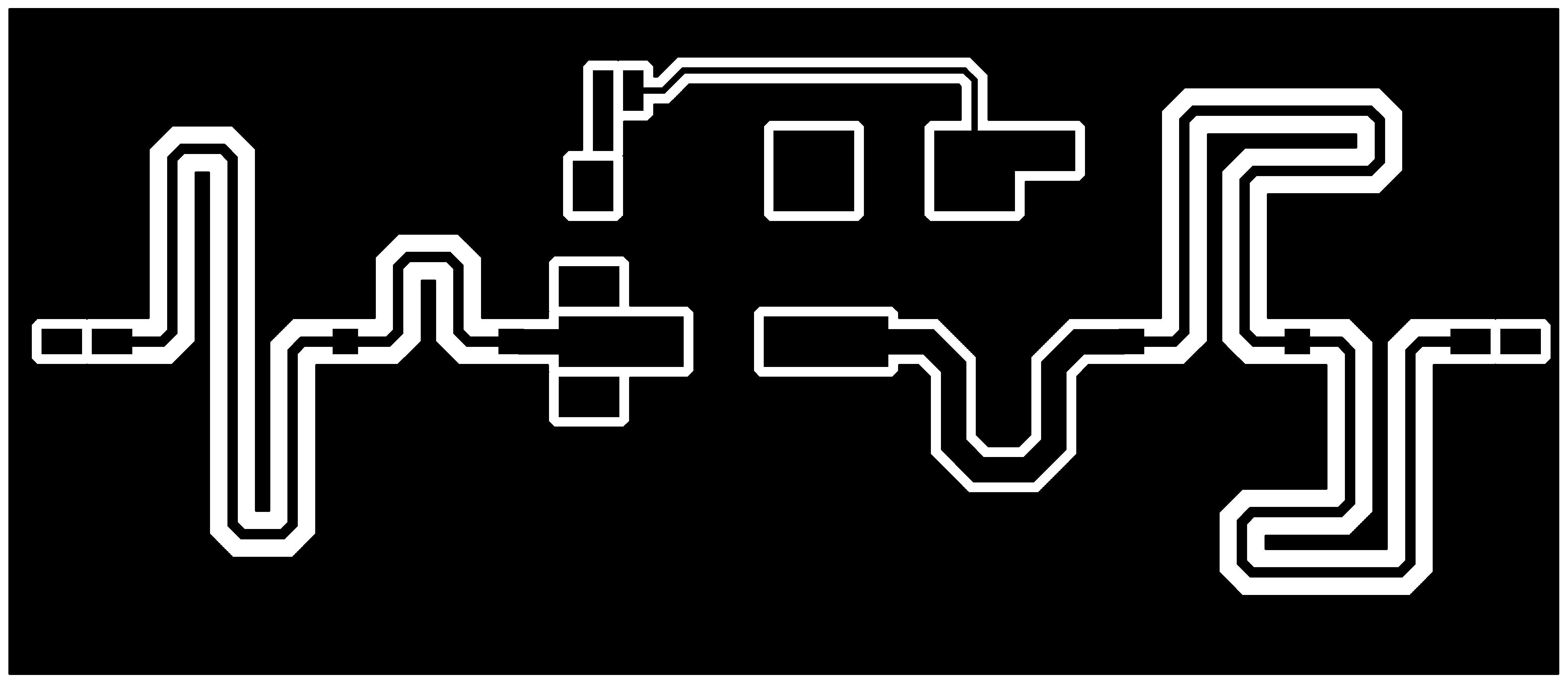
Top-side artwork as printed from Eagle, for Teflon.
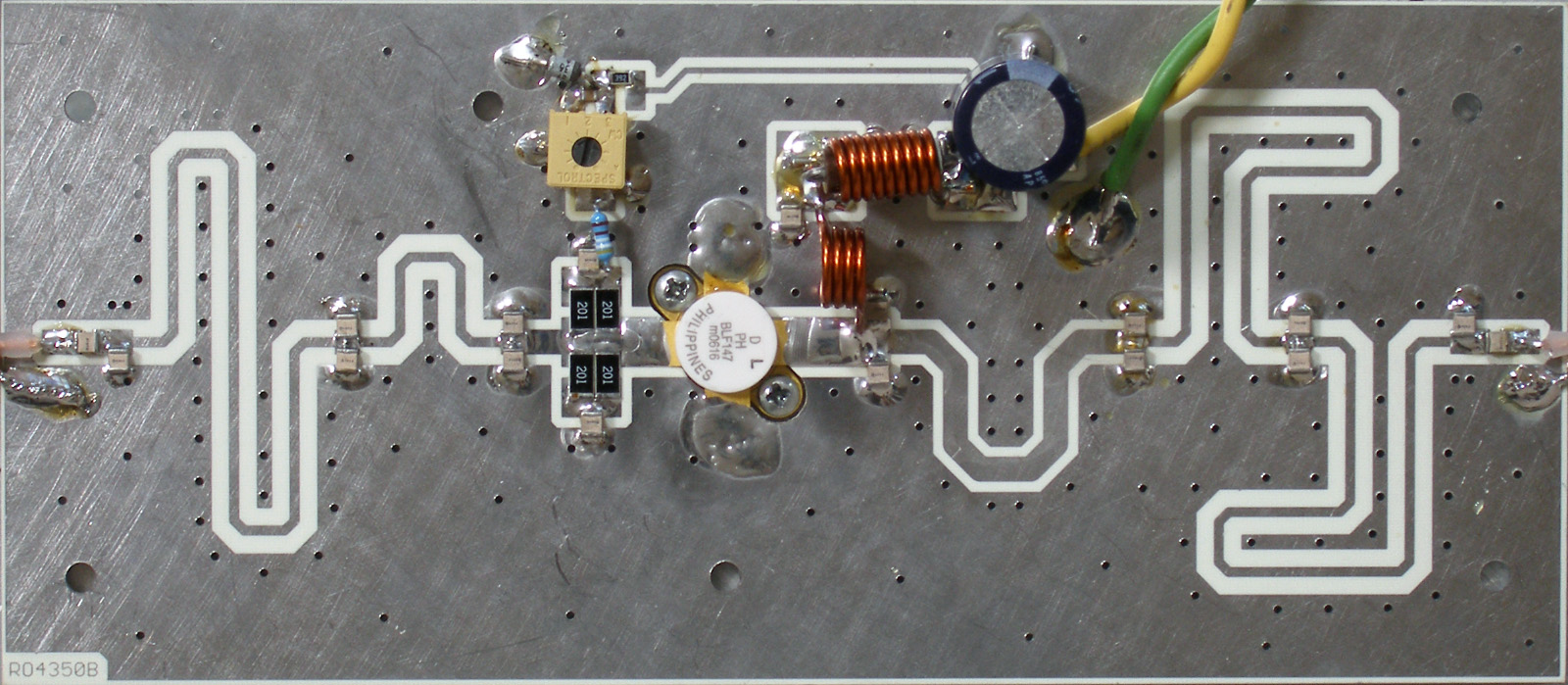
LATEST DEVELOPMENT: We are working with a version of this board on Rogers RO4350B. Results so far are encouraging - well over 150 W across the band with 10 W in and 24 VDC supply. Over 200 W at 28 VDC, and over 250 W with a hot bias (~ 4 or 5 A quiescent, as opposed to the usual 1 A). Trace dimensions are not the same as those for the Teflon board due to the higher dielectric constant. Photo:
Some design notes:
* All caps are ATC
100B family 1111 porcelain
caps. It's absolutely essential to use porcelain caps on the output,
and it's a very good idea for the input. The only recommendable
substitutes
would be the Dielectric Labs
C17AH series or the AVX porcelain
caps
(the SQCB family), which (unlike the ATC parts) do appear to
be
available from the distributors. As far as we can tell, they are
inferior to the ATC caps, although the C17s and SQCBs should be
fine at least
for the RF bypassing.
* Input and output coupling caps are 470 pF. That is a critical value.
* Input stage:
single 33 pF shunt at input
100 pF + 82 pF shunt at 2nd stage
330 pF x 2 shunt at 3rd stage
200 ohms x 4 (1 W, 2512) shunt to bypass at FET gate
bypass of the gate shunt resistors is 680 pF on each leg (value is not critical, so this can vary a little as needed)
* Output stage:
100 nH bias inductor - consists of about 5" of #16 enameled wire, wound with 4 turns with a 300 mil ID.
330 pF x 2 shunt at 1st stage
120 pF + 100 pF shunt at 2nd stage
27 pF x 2 shunt at 3rd stage
single 10 pF shunt at output
* The shunt cap placement is fairly critical. Caps should be placed centered on the pairs of 75-mil-spaced vias adjacent the cap pads.
* Bypass caps for the power pads are not super-critical - we used a few 680 pF to 1000 pF porcelain on the prototypes, whatever we had extra of.
* Gate bias is set so that the quiescent drain current is around 1 A. The normal voltage seems to be around 3 V. To get this we used 3.9 k from the B+ input to a shunt Zener, a 1N4736A (a 6.8 V Zener - that's what we had sitting around). From there a 10 k pot to ground with the wiper as output, and a 4.99 k in series with the wiper to one set of the 200 ohm resistors. Values are *not* critical. You can use a regulator here instead - a regulator is probably not necessary, but if you do use one, make sure you have some series resistance and some bypass capacitance to filter out reference noise.
* The power input filter cap is a 1000 uF 35 V cap - again, it's what we had sitting around, but it's a reasonable value. The choke between that pad and the drain bias inductor pad is 8 turns of #16 wire wrapped around something like a 200 ohm 1 W resistor - our version of a choke, but probably a ferrite is better. Likely neither of these component values is critical; you should use what you're comfortable with.
* Depending on how much power you put into this board, you may want to throttle back the VDD to 24 V instead of 28 V. With 10 W of drive we get close to 200 W out at 28 V, which is probably stressing the design just a bit. 24 V will give you around 150 W with 10 W in. At 13.8 V, we get 60 or 70 W out. Your mileage may vary.